The Core Insight: One Number, Two Perspectives
The density of silicon is often presented as a basic material property, but in engineering and procurement it carries broader meaning. It influences weight estimates, structural assumptions, wafer quality expectations, packaging compatibility, and material verification.
For buyers and engineers, the most commonly referenced value is the density of monocrystalline silicon, which is approximately 2.3290 g/cm³ under standard conditions.
This guide explains where that number comes from, why real materials may vary slightly from it, and why silicon density matters in design, manufacturing, and sourcing decisions.
Why Silicon Has That Density
Silicon’s density is not arbitrary. It comes from the relationship between atomic mass and how silicon atoms are arranged in the solid crystal.
Crystal Structure Matters
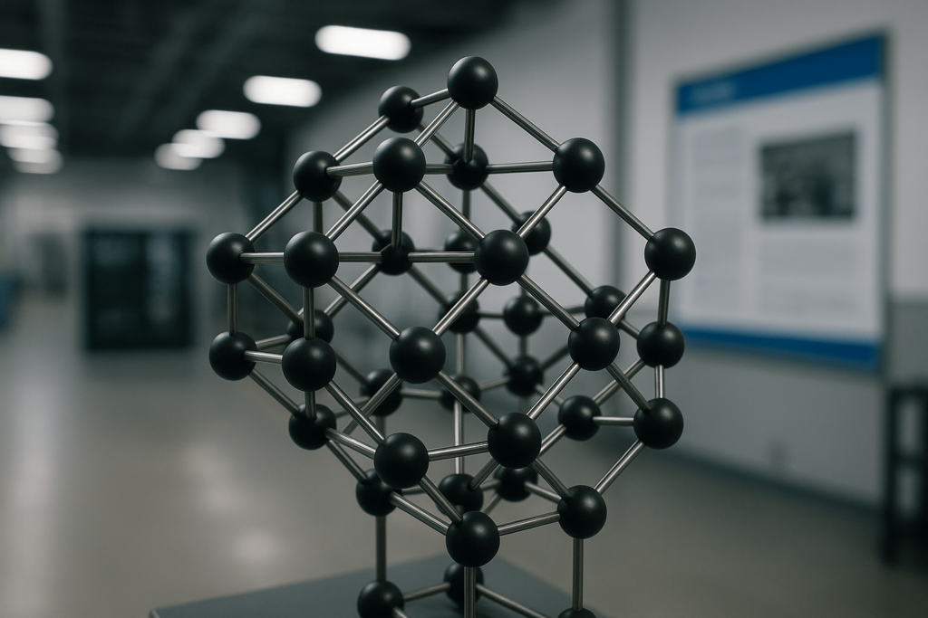
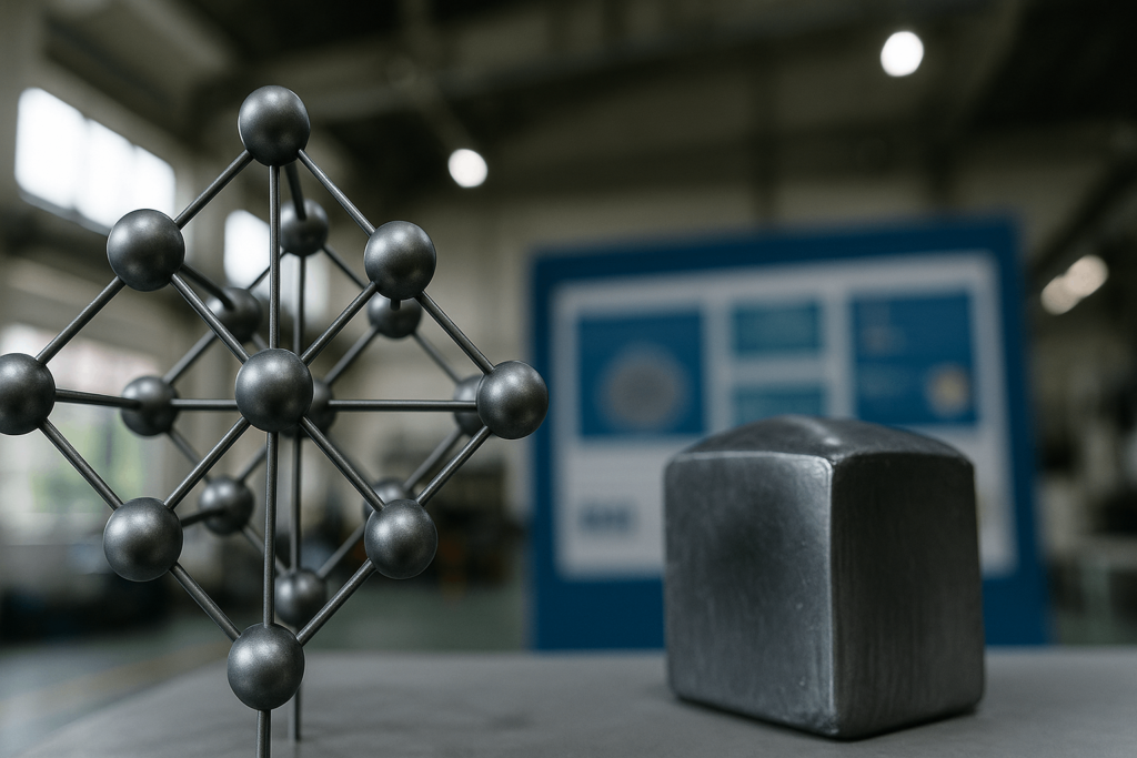
Monocrystalline silicon adopts a diamond cubic structure. This lattice is less densely packed than many common metallic crystal structures, which helps explain why silicon’s density is much lower than that of metals such as steel or copper.

Why the Calculation Works
In simplified terms, silicon density can be derived from:
the number of atoms in the unit cell;
the atomic mass of silicon;
the lattice constant that defines the cell volume.
This is why the theoretical density of monocrystalline silicon aligns closely with the commonly cited value of about 2.3290 g/cm³.

The Difference Between Theoretical and Bulk Density
A key distinction in materials engineering is the difference between theoretical density and bulk density.
theoretical density assumes a perfect crystal with no voids or structural defects;
bulk density reflects the material as it actually exists after processing, including imperfections such as vacancies, porosity, or microstructural irregularities.
For buyers, the gap between these values can matter because it may reflect purity, process quality, or the presence of internal defects. A small deviation may be normal, but larger deviations can suggest material or manufacturing issues that deserve review.
When Silicon Density Changes in Practice
Although silicon density is often treated as a fixed property, real materials do not always behave as perfectly constant systems.
Temperature and Pressure Effects
Temperature changes affect volume, and volume changes affect density. Silicon has a relatively low thermal expansion coefficient, which is one reason it is widely used in electronics and precision applications.
However, even small thermal-expansion differences become important when silicon is bonded to metals such as aluminum or copper. In packaging and hybrid assemblies, these mismatches can create stress even when the density value itself changes only slightly.

Different Forms of Silicon
Not all silicon materials have exactly the same density.
| Silicon Form | Approx. Density | Notes |
| Monocrystalline silicon | 2.3290 g/cm³ | Standard reference value |
| Polycrystalline silicon | ~2.3 g/cm³ | Slightly affected by grain structure |
| Amorphous silicon | ~2.285 g/cm³ | Lower due to less efficient packing |
| Porous silicon | Variable | Depends strongly on pore fraction and processing |
Doping and Internal Modification
Doping primarily changes electrical behavior, but it can also create slight structural distortion and small density shifts. These differences are often subtle, yet they matter in precision semiconductor and MEMS-related applications.
Why Silicon Density Matters to Buyers and Engineers
Silicon density matters because it affects more than weight. It can influence dimensional assumptions, packaging stress, transport calculations, and how accurately designers model a part or wafer in a larger system.
Common Engineering Consequences
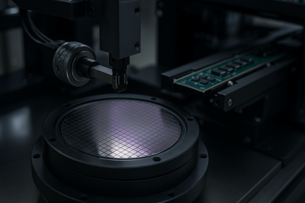
wafer uniformity affects downstream precision processes;
density and structure can influence MEMS and sensor behavior;
module or substrate weight affects logistics and support design;
density-related assumptions matter when silicon is combined with metals or polymers.

A Special Case: Measurement Science
Silicon density is also important in high-precision metrology, where extremely accurate material characterization has been used in fundamental measurement work. For most buyers, the practical lesson is simpler: if a material can be measured that precisely, then small deviations in production-grade material can also matter when the application is sensitive.
FAQ
What is the standard density of monocrystalline silicon?
The commonly cited value is approximately 2.3290 g/cm³ under standard conditions.
Is silicon denser than aluminum or steel?
No. Aluminum and steel are both denser than silicon.
What is the difference between silicon and silicone?
Silicon is an elemental semiconductor material. Silicone is a polymeric material with very different structure, behavior, and density.
Why is amorphous silicon less dense than monocrystalline silicon?
Because its atomic arrangement is less orderly and less efficiently packed.
Final Thoughts
The density of silicon is useful because it connects atomic structure with real engineering consequences. It is both a reference value and a signal of how material form, quality, and processing may affect performance.
For buyers and engineers, the most useful approach is to treat silicon density not as an isolated number, but as part of a wider material-verification and design-compatibility framework.


